Semiconductor Packaging
Beyond Traditional Packaging
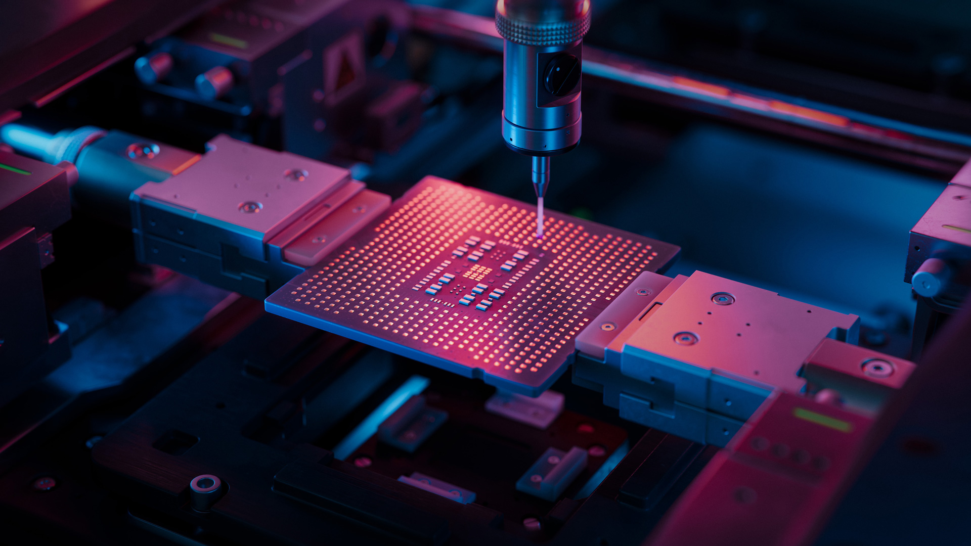
As semiconductor performance advances, packaging has become the limiting factor in system capability. Higher transistor density, chiplet architectures, 3D integration, and increasing power loads demand interconnect solutions that go beyond the constraints of traditional PCB and solder-based packaging.
The Occam Process provides a solderless, additive-enabled architecture that integrates components directly into a structurally reinforced substrate—forming direct metallurgical bonds that outperform solder in thermal, mechanical, and electrical performance.
Chiplet & Heterogeneous Integration
Modern semiconductor design is shifting toward chiplet-based architectures to improve yield, scalability, and modularity. However, chiplet performance depends heavily on interconnect density and signal integrity.
The Occam Process supports advanced integration by enabling:
- High-density interconnect routing
- Embedded die and packaged components
- Reduced interconnect length
- Improved signal integrity
- Flexible system partitioning
By building the structure around components rather than forcing them onto a fixed PCB, Occam enables greater architectural freedom for heterogeneous integration.
2.5D & 3D Architectures
As system performance scales, vertical integration becomes increasingly important. Occam’s additive interconnect methodology supports multilayer build-ups and compact 3D configurations without the thermal and mechanical weaknesses of solder joints.
This enables:
- Compact vertical stacking
- Improved thermal pathways
- Reduced parasitics
- Greater functional density
The result is packaging that supports high-performance computing, AI accelerators, and advanced system-in-package (SiP) designs.
Direct Metallurgical Bonding
Traditional packaging relies on solder bumps, balls, or reflow processes that introduce variability and long-term fatigue risk. Occam replaces these interconnects with direct metallurgical bonds formed through additive metallization techniques.
Advantages include:
- Superior thermal conductivity
- Higher mechanical strength
- Reduced interconnect resistance
- Elimination of solder fatigue
This approach increases lifecycle reliability while improving electrical and thermal efficiency.
Additive & MSAP Compatibility
The Occam Process aligns with advanced additive and semi-additive manufacturing techniques, including compatibility with Modified Semi-Additive Process (MSAP) methodologies.
This supports:
- Fine-line geometries
- Advanced routing density
- Reduced material waste
- Scalable next-generation manufacturing
- By integrating with modern fabrication strategies, Occam positions semiconductor packaging for long-term evolution beyond subtractive PCB processes.
Thermal & Power Density Advantage
As chip power densities increase, heat removal becomes one of the primary design challenges. Solder interconnects can limit thermal transfer efficiency, particularly in high-power devices.
Occam’s architecture improves thermal performance through:
- Direct conductive pathways
- Reduced interfacial resistance
- Structural heat distribution
- Lower junction temperatures
This enables higher sustained performance while protecting device longevity.
A Platform for the Future of Integration
Semiconductor innovation increasingly depends on packaging innovation. The Occam Process provides a solderless foundation for next-generation integration strategies, from chiplets to 3D assemblies and beyond.
By eliminating legacy interconnect limitations and enabling additive, high-density architectures, Occam supports the continued scaling of electronic performance in a post-solder era.